
The world of nanotechnology brings extraordinary possibilities, but working with devices measured in billionths of a meter requires specialized knowledge and careful handling to ensure both safety and optimal performance.
🔬 Understanding the Microscopic Universe of Nano Devices
Nano devices represent a revolutionary leap in technology, operating at scales between 1 and 100 nanometers. To put this in perspective, a single human hair is approximately 80,000 nanometers wide. These incredibly small instruments are transforming industries from medicine to electronics, but their tiny size creates unique challenges for handling, storage, and operation.
The field of nanotechnology has expanded rapidly over the past two decades, with applications ranging from targeted drug delivery systems to quantum computing components. As these devices become more prevalent in research laboratories, manufacturing facilities, and even consumer products, understanding proper handling techniques becomes increasingly critical for professionals across multiple sectors.
Unlike traditional electronic components or mechanical devices, nano-scale equipment requires specialized protocols that account for their sensitivity to environmental conditions, ease of contamination, and potential health implications. The stakes are high—improper handling can destroy expensive equipment, compromise research results, or even pose health risks to handlers.
⚠️ Recognizing the Hidden Risks of Nano-Scale Work
Working with nano devices introduces hazards that aren’t immediately apparent to those accustomed to handling conventional equipment. The primary concern stems from the unique physical and chemical properties that materials exhibit at the nanoscale, which often differ dramatically from their bulk counterparts.
Nanoparticles can potentially penetrate biological barriers that normally protect the human body, including skin, lungs, and even the blood-brain barrier. While research into the long-term health effects is ongoing, current evidence suggests that certain nanomaterials may cause inflammation, oxidative stress, or other biological responses when exposure occurs without proper protection.
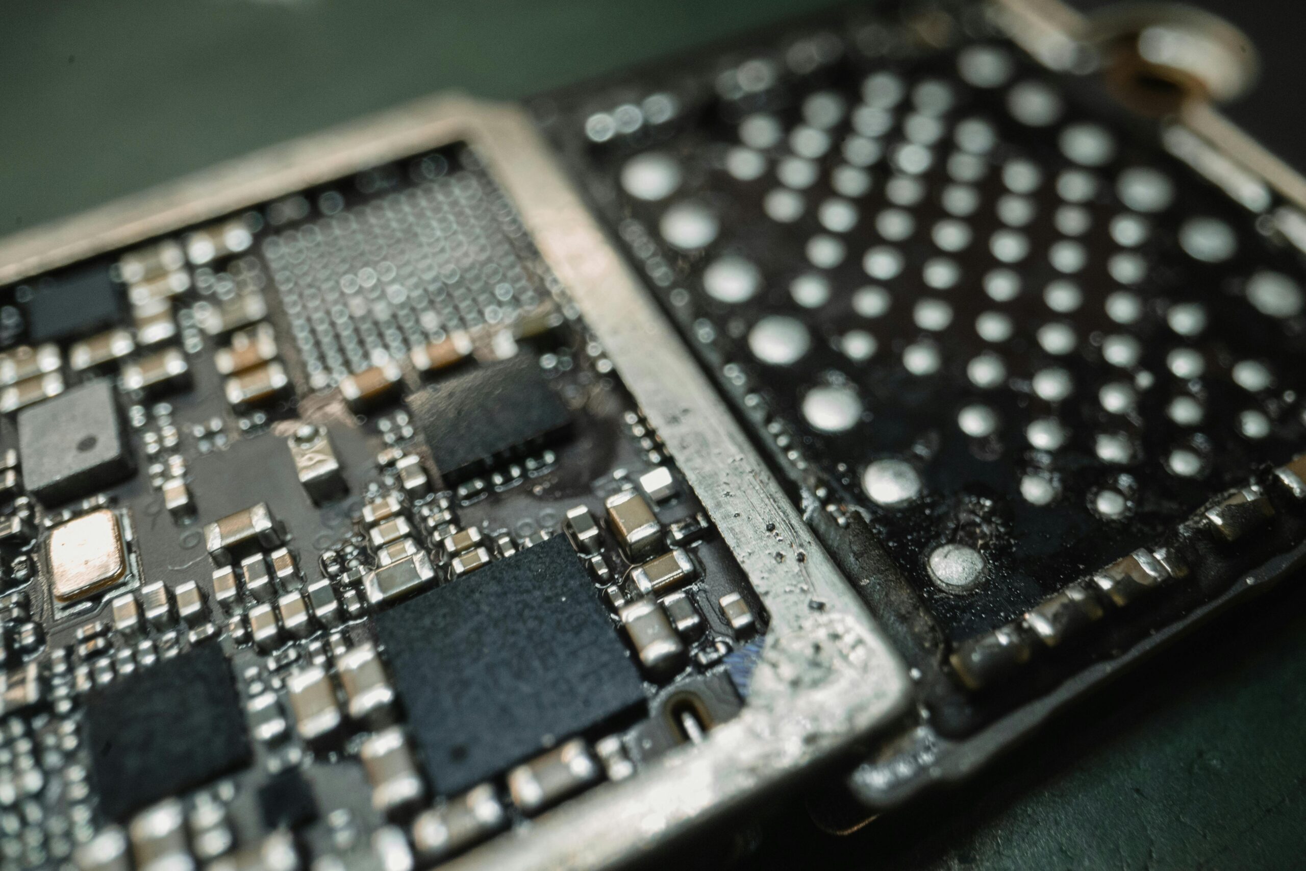
Environmental contamination represents another significant risk. Nano devices are extraordinarily sensitive to dust, moisture, electromagnetic interference, and even slight vibrations. A single particle of ordinary dust—massive by comparison—can damage or destroy nano-scale circuitry. Static electricity that you might not even notice can generate devastating electrical discharges at the nano level.
Common Contamination Sources to Avoid
- Airborne particulates from unfiltered environments
- Oils and residues from ungloved hands
- Moisture from breath or humid conditions
- Chemical vapors from cleaning products or solvents
- Electromagnetic interference from nearby equipment
- Mechanical vibrations from HVAC systems or foot traffic
🧤 Essential Personal Protective Equipment for Nano Handling
The foundation of safe nano device handling begins with appropriate personal protective equipment. Unlike standard laboratory or manufacturing environments, working with nanomaterials requires specialized gear designed to provide protection both ways—protecting you from the materials and protecting the materials from contamination.
Nitrile gloves are the minimum requirement, but powder-free versions are essential since powder residues can contaminate nano devices. Many facilities require double-gloving for added protection and contamination control. The gloves should fit properly without being too loose, as excess material can accidentally contact sensitive equipment.
Eye protection is non-negotiable when handling nanomaterials, particularly in powder form. Safety glasses or goggles prevent accidental exposure through the eyes and protect against potential splashes during liquid-phase work. For environments with airborne nanoparticle risks, full face shields provide comprehensive protection.
Respiratory protection deserves special attention. Standard dust masks are insufficient for nano-scale particles. N95 respirators represent the minimum acceptable standard, though many facilities require N99 or even N100 respirators when working with potentially hazardous nanomaterials. Proper fit testing ensures that these respirators provide the intended protection level.
Laboratory coats or cleanroom suits prevent contamination transfer between your clothing and the work environment. These garments should be made from low-particle-generating materials and laundered or disposed of according to facility protocols. In cleanroom environments, full bunny suits with integrated hoods may be required to maintain the necessary contamination control standards.
🏢 Creating the Optimal Environment for Nano Work
The workspace where you handle nano devices matters as much as the handling techniques themselves. Professional-grade cleanrooms represent the gold standard, but even modest improvements to standard laboratory environments can significantly reduce contamination risks and improve outcomes.
HEPA filtration systems remove 99.97% of particles 0.3 microns and larger from the air, creating a substantially cleaner environment than standard rooms. While this doesn’t eliminate nanoparticles entirely, it dramatically reduces the particulate load that could damage sensitive devices. Portable HEPA filters offer a cost-effective solution for laboratories that cannot install permanent cleanroom infrastructure.
Temperature and humidity control prevents condensation and reduces static electricity buildup. Most nano device handling should occur at 20-22°C with relative humidity between 40-60%. These conditions minimize moisture-related damage while keeping static discharge risks manageable. Digital hygrometers and thermometers help maintain awareness of environmental conditions.
Vibration isolation becomes critical when working with nano-scale equipment. Optical tables with pneumatic isolation systems effectively dampen vibrations from building systems, foot traffic, and nearby equipment. For less critical applications, simply locating workstations away from high-traffic areas and mechanical equipment reduces vibration exposure.
Electromagnetic Shielding Considerations
Nano electronic devices are extraordinarily sensitive to electromagnetic interference. Faraday cages or shielded enclosures protect sensitive work from radio frequency interference, while proper grounding prevents static buildup. Mobile phones, wireless devices, and even LED lighting can generate sufficient electromagnetic noise to affect nano-scale measurements or damage sensitive components.
🔧 Mastering Precision Handling Techniques
The actual manipulation of nano devices requires skills and techniques quite different from conventional electronics or mechanical work. Visualization itself presents the first challenge—nano devices are too small to see with the naked eye, requiring specialized microscopy equipment for observation and manipulation.
Micromanipulators provide the precision control necessary for positioning and assembling nano devices. These instruments translate relatively large hand movements into extremely fine positioning adjustments measured in micrometers or nanometers. Learning to operate micromanipulators effectively requires practice and patience, as the hand-eye coordination differs significantly from normal manipulation tasks.
When transferring nano devices between locations or storage containers, always work under appropriate magnification. Optical microscopes, scanning electron microscopes, or atomic force microscopes allow visual confirmation of device position and condition. Never assume a nano device is where you think it is without visual verification—these objects are so small they can easily be lost or displaced by air currents.
Specialized tools replace traditional tweezers and probes when working at the nanoscale. Vacuum pickup tools use gentle suction to lift and position delicate structures without mechanical contact that could cause damage. Electrostatic pickup systems offer another non-contact manipulation method, though these require careful ESD control to prevent discharge damage.
📦 Storage and Transportation Best Practices
Proper storage protects nano devices from environmental degradation between handling sessions. Specialized containers maintain controlled atmospheres that prevent oxidation, moisture exposure, and contamination. Desiccant-filled cases with sealed gaskets provide cost-effective protection for many applications.
Nitrogen purging creates an inert atmosphere that prevents oxidation of sensitive materials. Small nitrogen-purged storage cabinets maintain this protective environment continuously, while portable nitrogen-purged containers enable safe transportation. For extremely sensitive materials, vacuum storage eliminates atmospheric exposure entirely.
Labeling and organization prevent confusion and reduce unnecessary handling. Clear identification systems ensure that devices can be located without extensive searching through multiple containers. Inventory management systems, whether simple spreadsheets or sophisticated database applications, track device locations, handling history, and storage conditions.
Transportation of nano devices requires additional precautions beyond static storage. Shock-absorbing packaging protects against mechanical impacts, while moisture barrier bags prevent humidity exposure during transit. For shipping, specialized carriers experienced in handling sensitive scientific equipment provide the necessary care and chain-of-custody documentation.
🧪 Contamination Prevention and Cleaning Protocols
Despite best efforts, contamination sometimes occurs during nano device handling. Having effective cleaning protocols enables recovery of contaminated devices rather than disposal. However, cleaning nanoscale structures requires extreme care—aggressive cleaning methods can easily destroy the devices you’re trying to save.
Solvent cleaning represents the most common approach for removing organic contamination. Isopropyl alcohol, acetone, and specialized electronic-grade solvents can remove oils, residues, and some particulates. The key is using high-purity solvents that won’t leave their own residues behind. Immersion cleaning, spray cleaning, or vapor degreasing may be appropriate depending on device design and contamination type.
Plasma cleaning uses ionized gas to remove organic contamination without mechanical contact or liquid solvents. Oxygen plasma effectively removes hydrocarbon contamination, while other plasma chemistries address specific contaminant types. This method is particularly valuable for delicate nanostructures that cannot withstand aggressive solvent or mechanical cleaning.
UV-ozone cleaning combines ultraviolet light with ozone generation to break down organic contaminants. This technique works well for surface cleaning without physical contact or harsh chemicals. However, some materials may be sensitive to UV exposure, requiring careful consideration before applying this method.
⚡ Electrostatic Discharge Protection Strategies
Electrostatic discharge poses one of the most insidious threats to nano electronic devices. Voltages that humans cannot even detect can permanently damage nanoscale circuitry. Comprehensive ESD protection requires multiple layers of defense working together to prevent charge buildup and provide safe discharge paths.
ESD-safe work surfaces form the foundation of electrostatic protection. Conductive or dissipative mats connected to proper grounding points allow static charges to dissipate safely rather than accumulating until discharge occurs. These mats must be regularly tested to ensure they maintain appropriate electrical properties—worn or contaminated mats lose their protective capabilities.
Wrist straps provide a continuous grounding path from the operator to earth ground. Properly worn and connected wrist straps prevent charge buildup on the handler’s body that could discharge through sensitive devices. Regular testing with dedicated wrist strap testers ensures these safety devices function correctly.
Ionizers actively neutralize static charges in the air surrounding the work area. These devices generate balanced streams of positive and negative ions that neutralize charged surfaces within their effective range. Ionizers are particularly valuable when handling insulating materials that cannot be grounded directly, as they provide charge neutralization without physical contact.
📊 Quality Control and Verification Methods
Confirming that nano devices remain functional and uncontaminated after handling requires appropriate inspection and testing protocols. Visual inspection under magnification provides the first line of defense, revealing obvious contamination, mechanical damage, or positioning errors.
Electrical testing verifies the functionality of nano electronic devices. Specialized probe stations with micro-positioners enable electrical contact with nanoscale features for resistance measurements, I-V characterization, or functional testing. These measurements confirm that handling procedures have not degraded device performance.
Advanced characterization techniques provide deeper insights into device condition. Scanning electron microscopy reveals structural details far beyond optical microscope capabilities, while atomic force microscopy maps surface topography at the atomic level. X-ray photoelectron spectroscopy identifies surface contamination by chemical composition.
| Inspection Method | Resolution | Best Application |
|---|---|---|
| Optical Microscopy | ~200 nm | Quick visual inspection |
| Scanning Electron Microscopy | ~1 nm | Structural analysis |
| Atomic Force Microscopy | ~0.1 nm | Surface topography |
| Electrical Testing | Function-dependent | Performance verification |
👥 Training and Skill Development for Nano Handling
Competent handling of nano devices requires training that goes beyond traditional laboratory skills. Organizations should implement structured training programs that combine theoretical knowledge with hands-on practice under supervision. Starting with larger-scale practice devices allows skill development without risking expensive nanoscale equipment.
Mentorship from experienced practitioners accelerates learning and helps newcomers avoid common mistakes. Pairing new handlers with veterans provides opportunities to observe proper techniques and receive immediate feedback on performance. This apprenticeship model has proven effective across many technical disciplines.
Regular refresher training maintains skills and introduces new techniques or equipment. The nanotechnology field evolves rapidly, with new handling methods, tools, and best practices emerging continuously. Staying current requires ongoing education through workshops, conferences, technical literature, and professional development courses.
Documentation of procedures ensures consistency across different operators and shifts. Standard operating procedures capture institutional knowledge in written form, providing reference material for both training and daily operations. Video documentation can be particularly valuable for demonstrating complex manipulation techniques that are difficult to describe in text alone.
🌍 Environmental and Disposal Considerations
Responsible nano device handling extends to end-of-life disposal and environmental impact management. Many nanomaterials require special disposal procedures rather than treatment as standard laboratory waste. Understanding regulatory requirements and best practices protects both environmental and human health.
Waste segregation separates different types of nanomaterials to prevent incompatible materials from mixing. Clearly labeled waste containers with appropriate hazard warnings ensure proper handling throughout the disposal chain. Liquid wastes, solid wastes, and contaminated personal protective equipment often require separate disposal streams.
Some nanomaterials can be recycled or reclaimed rather than disposed of entirely. Precious metal nanoparticles, for example, may have sufficient value to justify recovery and recycling. Contacting specialized waste management companies that handle nanomaterials provides guidance on recycling opportunities and proper disposal methods.
💡 Staying Ahead with Emerging Technologies and Methods
The rapid pace of nanotechnology development means that handling techniques continue to evolve. Automation and robotics are increasingly being applied to nano device manipulation, reducing human exposure while improving precision and repeatability. Collaborative robots designed for cleanroom environments can perform repetitive handling tasks with superhuman consistency.
Artificial intelligence and machine vision systems assist with nano device positioning and inspection. These technologies can identify defects, verify positioning, and even suggest optimal handling strategies based on device characteristics. As these tools mature, they will likely become standard components of nano handling workflows.
Remote operation systems enable manipulation of nano devices from outside cleanroom environments or even off-site locations. This approach reduces contamination risks while allowing experts to assist with handling tasks regardless of physical location. Haptic feedback systems provide the operator with tactile sensations that improve manipulation precision despite the remote interface.
🎯 Building Your Nano Handling Excellence
Mastering nano device handling represents a journey rather than a destination. Each handling session provides opportunities to refine techniques, identify potential improvements, and deepen understanding of these remarkable technologies. Success requires patience, attention to detail, and commitment to continuous improvement.
Starting with proper equipment, training, and procedures establishes a strong foundation. As experience grows, handlers develop intuition about how nano devices respond to different conditions and manipulations. This expertise becomes invaluable when troubleshooting unexpected issues or working with novel device types.
Collaboration within the nanotechnology community accelerates collective progress. Sharing experiences, challenges, and solutions through professional networks, conferences, and publications helps everyone improve their practices. The field benefits when practitioners openly discuss both successes and failures, as both provide valuable learning opportunities.
The extraordinary capabilities of nano devices justify the care and precision required for their handling. From revolutionary medical treatments to quantum computing breakthroughs, nanotechnology promises to transform our world in profound ways. By mastering the essential techniques for safe handling of these tiny devices, you position yourself at the forefront of this technological revolution, contributing to discoveries and innovations that were impossible just decades ago.
Remember that safety, precision, and contamination control form the three pillars of effective nano device handling. Neglecting any of these elements compromises results and potentially puts handlers at risk. With proper attention to these fundamentals, combined with ongoing skill development and awareness of emerging best practices, you can confidently navigate the nano world and unlock its tremendous potential. 🚀