
Nano-films are revolutionizing how we perceive transparency in modern technology, combining cutting-edge science with practical applications that enhance our daily lives.
🔬 The Science Behind Transparent Nano-Films
Transparency in nano-films represents one of the most fascinating achievements in materials science. These ultra-thin coatings, measuring just billionths of a meter in thickness, have transformed industries ranging from electronics to architecture. The fundamental principle behind their optical clarity lies in their ability to manipulate light at the nanoscale, creating surfaces that are virtually invisible while providing enhanced functionality.
At the molecular level, nano-films are engineered to minimize light scattering and absorption. Traditional materials often appear opaque or translucent because their internal structures interfere with light waves passing through them. However, nano-films are designed with such precision that their components are smaller than the wavelength of visible light, typically ranging from 400 to 700 nanometers. This dimensional relationship is crucial—when structures are smaller than light wavelengths, they become essentially invisible to the human eye.
The refractive index matching is another critical factor in achieving optical clarity. Scientists carefully select materials and optimize their composition to ensure that the nano-film’s refractive index closely matches the substrate beneath it. This minimizes reflection at the interface, allowing light to pass through seamlessly. Advanced deposition techniques like atomic layer deposition (ALD) and chemical vapor deposition (CVD) enable manufacturers to build these films atom by atom, ensuring unprecedented uniformity and clarity.
✨ Applications Transforming Modern Technology
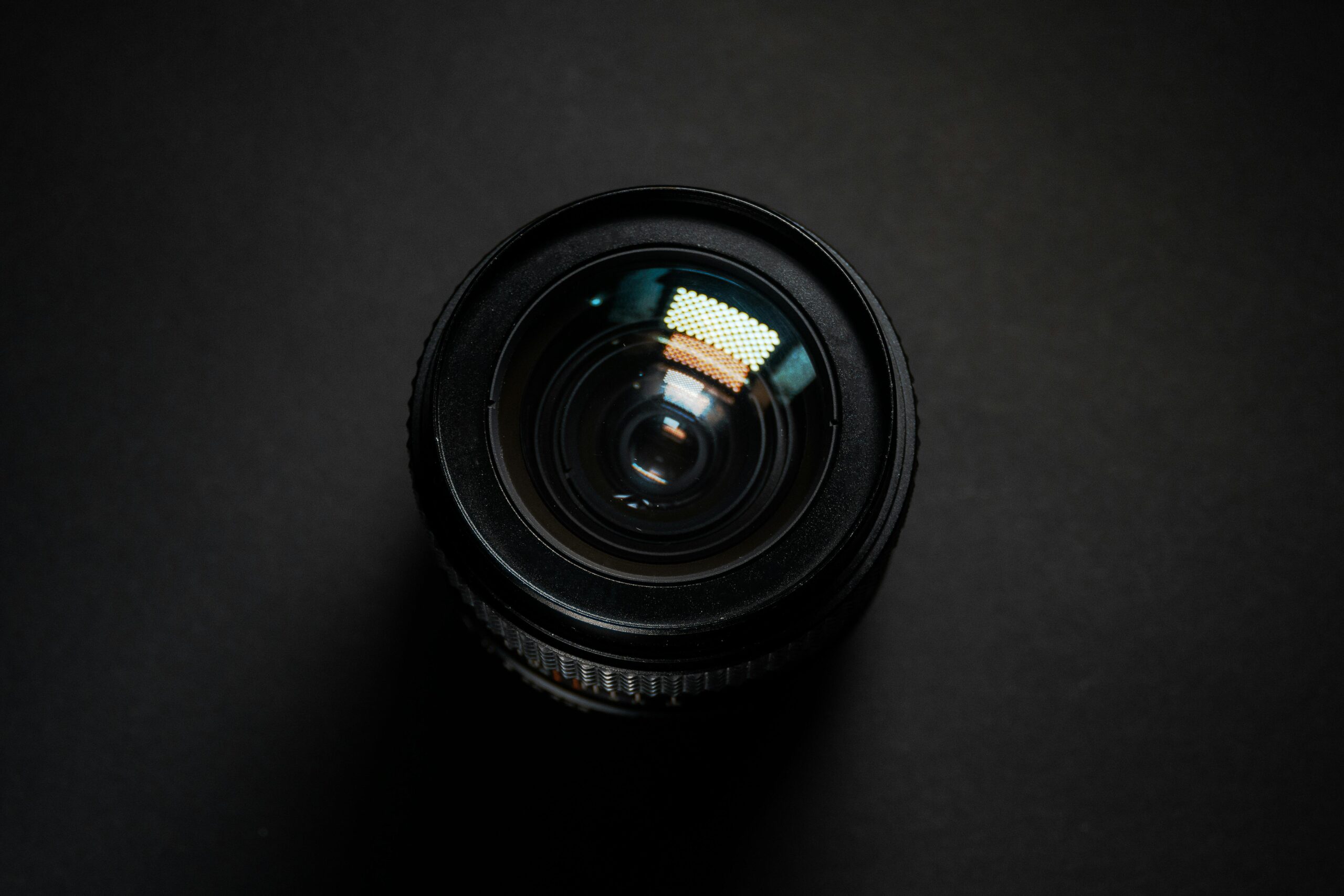
The practical applications of transparent nano-films extend far beyond laboratory curiosity. In the smartphone industry, these films serve as protective layers that are virtually undetectable, safeguarding delicate display panels without compromising visual quality. Anti-fingerprint coatings, scratch-resistant layers, and anti-reflective surfaces all rely on nano-film technology to maintain the crystal-clear displays consumers demand.
Architectural glass has experienced a revolution thanks to nano-film coatings. Buildings can now feature windows that appear perfectly clear while blocking harmful UV radiation, reducing heat transmission, and even self-cleaning when exposed to sunlight. These smart glass solutions incorporate titanium dioxide nano-films that break down organic contaminants through photocatalytic reactions, keeping surfaces pristine with minimal maintenance.
In the automotive sector, transparent nano-films enhance both safety and aesthetics. Windshields treated with hydrophobic nano-coatings cause water to bead and roll off instantly, improving visibility during rain. Anti-fog treatments prevent condensation buildup, while UV-blocking films protect passengers without darkening the interior. These innovations demonstrate how transparency and functionality can coexist harmoniously.
🎯 Engineering Perfect Clarity: Materials and Methods
Creating transparent nano-films requires careful selection of base materials. Silicon dioxide, titanium dioxide, aluminum oxide, and various polymer compounds serve as primary building blocks. Each material offers distinct advantages: silicon dioxide provides excellent optical clarity and chemical stability, titanium dioxide offers photocatalytic properties, while aluminum oxide delivers superior hardness and scratch resistance.
The manufacturing process demands extreme precision. Physical vapor deposition (PVD) techniques allow manufacturers to evaporate source materials and condense them onto substrates in controlled environments. Magnetron sputtering, a specialized PVD method, uses magnetic fields to direct ionized particles onto surfaces, creating exceptionally uniform coatings. These processes occur in vacuum chambers where contamination is virtually eliminated, ensuring the purity essential for optical clarity.
Layer-by-layer assembly represents another sophisticated approach. Scientists alternate between depositing positively and negatively charged materials, building up nano-films through electrostatic attraction. This method offers remarkable control over film thickness and composition, enabling the creation of complex multi-layer structures with tailored optical properties. Some advanced films incorporate dozens of individual layers, each optimized for specific functions while maintaining overall transparency.
🌟 Overcoming Challenges in Nano-Film Development
Despite remarkable progress, achieving perfect transparency in nano-films presents ongoing challenges. Defects at the nanoscale can significantly impact optical performance. Even microscopic impurities, pinholes, or thickness variations can cause light scattering or create visible imperfections. Quality control systems must detect flaws measuring just a few nanometers—a task requiring sophisticated inspection equipment and rigorous testing protocols.
Durability represents another critical concern. While nano-films excel in laboratory conditions, real-world environments pose harsh tests. Temperature fluctuations, humidity, mechanical stress, and chemical exposure can all degrade film integrity over time. Researchers continuously work to enhance adhesion, improve resistance to environmental factors, and extend the functional lifespan of these coatings without compromising their transparency.
Cost considerations also influence development trajectories. Advanced deposition equipment requires substantial capital investment, and some processes demand rare or expensive materials. Scaling production from laboratory samples to commercial quantities introduces additional complexities. Balancing performance requirements with economic viability remains an ongoing challenge that shapes which nano-film technologies reach widespread adoption.
💡 The Role of Interference and Diffraction
Understanding light behavior at the nanoscale illuminates why these films achieve such remarkable clarity. Thin-film interference, a phenomenon where light waves reflect from both the top and bottom surfaces of a film, can either enhance or diminish transparency depending on film thickness and wavelength. Anti-reflective coatings exploit destructive interference, where reflected waves cancel each other out, maximizing light transmission.
Multi-layer interference coatings take this concept further by stacking multiple thin films with alternating refractive indices. Each layer is precisely engineered to create destructive interference for reflected light across the visible spectrum. The result is a coating that appears nearly invisible, transmitting more than 99% of incident light in some applications. This technology finds use in camera lenses, eyeglasses, and display screens where maximum clarity is paramount.
Diffraction effects become negligible when nano-film structures are sufficiently small. Unlike conventional materials with micron-scale features that scatter light and create haziness, properly engineered nano-films with sub-wavelength structures allow light to pass through unimpeded. This principle enables the creation of surfaces that are simultaneously functional and optically transparent—a combination previously thought impossible.
🔍 Testing and Characterizing Optical Properties
Measuring transparency in nano-films requires specialized instruments capable of detecting minute variations in optical performance. Spectrophotometers analyze how films transmit, reflect, and absorb light across different wavelengths, providing detailed spectral profiles. Transmission measurements reveal what percentage of light passes through, while haze measurements quantify diffuse scattering that can reduce apparent clarity.
Ellipsometry serves as a powerful technique for characterizing nano-film thickness and refractive index without damaging samples. This method analyzes changes in polarized light reflected from film surfaces, extracting detailed information about film properties with sub-nanometer precision. Such measurements are essential for quality control and for optimizing deposition processes to achieve target specifications.
Microscopy techniques including scanning electron microscopy (SEM) and atomic force microscopy (AFM) visualize nano-film surfaces at extremely high magnification. These tools reveal surface roughness, particle contamination, and structural uniformity—factors that critically influence optical clarity. Advanced imaging helps researchers understand how processing parameters affect final film quality and guides improvements in manufacturing techniques.
🌐 Future Horizons in Transparent Nano-Technology
The future of transparent nano-films promises even more impressive capabilities. Researchers are developing smart films that can dynamically adjust their properties in response to external stimuli. Electrochromic nano-films change transparency when voltage is applied, enabling windows that switch between clear and tinted states on demand. These technologies could revolutionize building energy efficiency by controlling solar heat gain throughout the day.
Flexible transparent nano-films are enabling new device form factors. Foldable smartphones and rollable displays rely on ultra-thin coatings that maintain optical clarity while withstanding repeated bending. Conductive transparent films made from materials like graphene or silver nanowires serve as flexible electrodes in next-generation touch screens and solar cells, combining electrical functionality with optical transparency.
Self-healing nano-films represent another frontier. Scientists are engineering coatings with polymer chains that can reconnect after being scratched or damaged, automatically restoring transparency. Some experimental films incorporate capsules containing repair materials that rupture when damage occurs, filling defects and maintaining film integrity. These innovations could dramatically extend the lifespan of protective coatings on consumer devices and architectural surfaces.
🏗️ Industrial Implementation and Market Growth
The transparent nano-film market has experienced explosive growth, driven by consumer electronics demand and expanding applications across industries. Market analysts project continued expansion as manufacturing costs decline and new applications emerge. Major technology companies invest heavily in nano-coating research, recognizing that superior display clarity and device durability provide competitive advantages.
Standardization efforts are helping to mature the industry. Organizations are developing testing protocols, performance specifications, and safety guidelines specific to nano-films. These standards facilitate comparison between products, build consumer confidence, and enable manufacturers to demonstrate compliance with industry requirements. As standards evolve, they’re accelerating adoption by reducing uncertainty for companies considering nano-film integration.
Environmental considerations are shaping development priorities. Manufacturers are exploring water-based deposition processes, recyclable coating materials, and energy-efficient production methods. Some companies have developed bio-based transparent films derived from sustainable sources like cellulose nanocrystals, offering comparable optical performance with reduced environmental impact. These green alternatives align with broader sustainability goals while maintaining the technical excellence customers expect.
🎨 Aesthetic and Functional Balance
Achieving transparency in nano-films isn’t solely about maximizing light transmission—it’s about creating surfaces that enhance human experience. Color neutrality ensures that films don’t introduce unwanted tints or color shifts. This requires careful material selection and precise control over film composition, as even slight variations can create perceptible color casts that detract from visual quality.
Surface smoothness contributes significantly to perceived clarity. Nano-films with atomically smooth surfaces eliminate light scattering that would otherwise create haze or cloudiness. Advanced polishing and deposition techniques produce surfaces with roughness measured in single-digit nanometers, approaching theoretical smoothness limits. This exceptional flatness allows light to interface cleanly with the film, preserving image sharpness and contrast.
Glare reduction enhances both aesthetics and functionality. Matte nano-textured surfaces scatter reflected light in controlled patterns, reducing distracting reflections without significantly diminishing transmission. This approach proves particularly valuable for displays viewed in bright environments, where conventional glossy surfaces become mirrors. By engineering surface textures at the nanoscale, designers achieve anti-glare properties while maintaining overall transparency.
⚡ Performance Metrics That Matter
Quantifying nano-film performance requires examining multiple parameters beyond simple transparency percentages. Total light transmission indicates how much visible light passes through, but spectral selectivity reveals performance across different wavelengths. Some applications prioritize visible light transmission while blocking infrared or ultraviolet radiation, requiring films with wavelength-specific properties.
Durability testing subjects nano-films to accelerated aging conditions that simulate years of real-world exposure. Abrasion resistance, chemical stability, temperature cycling, and humidity exposure all factor into performance evaluations. Films must maintain optical clarity throughout their intended lifespan despite environmental stresses that would degrade lesser coatings. Standardized tests help manufacturers and customers alike understand long-term performance expectations.
Contact angle measurements assess hydrophobic or hydrophilic properties that influence how water and contaminants interact with surfaces. High contact angles indicate water beads up and rolls off easily, keeping surfaces cleaner. Low contact angles suggest surfaces spread water into thin films that evaporate quickly. These characteristics significantly impact perceived clarity in outdoor applications where rain, condensation, or cleaning affect visual appearance.
🚀 Pushing Boundaries: Emerging Research Directions
Academic and industrial laboratories continue pushing the boundaries of what’s possible with transparent nano-films. Metamaterial approaches use precisely patterned nanostructures to achieve optical properties impossible with conventional materials. These engineered surfaces can bend light in unusual ways, creating lenses, diffusers, or beam-shaping elements that are completely flat and transparent—opening new possibilities for compact optical systems.
Quantum dot incorporation into transparent matrices enables films with unique luminescent properties. These nano-films can absorb one wavelength of light and emit another, converting harmful UV radiation into visible light or enhancing display color gamut. Agricultural applications use these films in greenhouses to optimize the light spectrum for plant growth while maintaining transparency for natural illumination.
Bio-inspired designs draw lessons from nature’s transparent structures. Researchers study corneas, fish scales, and insect wings to understand how biological systems achieve remarkable clarity with organic materials. Biomimetic nano-films replicate these natural strategies, creating coatings that are simultaneously transparent, self-cleaning, anti-reflective, and mechanically robust. Nature’s billions of years of evolution provide a rich source of inspiration for engineering breakthroughs.
The journey toward perfect transparency in nano-films continues to advance through scientific innovation, engineering precision, and creative problem-solving. As researchers overcome current limitations and discover new possibilities, these invisible coatings will become even more integral to technologies shaping our visual experience. The art of creating crystal-clear nano-films combines fundamental physics, advanced chemistry, and meticulous manufacturing—a truly multidisciplinary achievement that makes the complex appear beautifully simple. From the screens we touch daily to the windows through which we view the world, transparent nano-films enhance clarity while adding functionality we increasingly take for granted, proving that the most sophisticated technologies are often the ones we never notice at all.